


There is a tidy story circulating in technology trade press about Qualcomm's November 2026 announcement: the company validated its High Bandwidth Compute silicon, achieved an 18-fold increase in memory bandwidth, and is now on a clear path to transforming AI inference economics. The headline numbers are striking. The timing is convenient. And for data center infrastructure teams evaluating next-generation accelerators, the temptation is to file this under "promising but early" and move on.
But the actual story buried in Qualcomm's technical disclosures is more nuanced and more useful for practitioners who need to make purchasing decisions in 2027 and beyond. The 18x figure exists, but so does a footnote. The validation happened, but in a specific configuration that differs from what customers will actually deploy. The efficiency gains are real, but they arrived slightly below Qualcomm's own projections. Understanding what was actually measured versus what was estimated matters, because the gap between those two numbers is precisely where data center buyers need to focus their scrutiny.
The 18x Claim: Total Bandwidth, Not Module Bandwidth
Qualcomm's HBC Gen 1 achieved 133 terabytes per second of total memory bandwidth on the AI250 accelerator card, representing an 18-fold increase over the LPDDR5X memory currently used in the AI200 card. Those are the headline numbers, and they are genuinely significant. But the sources are careful to specify that this is a total accelerator memory bandwidth number, not a per-HBC module bandwidth figure. That distinction matters for data center buyers running different configurations or evaluating scaling scenarios.
According to TechPowerUp's coverage of the validation announcement, the measurement reflects the complete accelerator card's memory subsystem performance rather than the performance of an individual HBC stacking module. For procurement teams calculating bandwidth-per-rack-unit or bandwidth-per-dollar, this distinction affects how the figure translates to actual deployment scenarios. A system integrator building a multi-card rack will achieve different aggregate numbers than a single-card evaluation.
The 133 TB/s figure also comes from a first-generation implementation using a two-layer DRAM stack. Qualcomm has stated that commercial products will employ a four-layer DRAM stack, effectively doubling the memory density and potentially altering the bandwidth profile. The company describes this as a viable roadmap for scaling across many Qualcomm AI accelerators, but the validation data does not yet reflect that production configuration. Early adopters evaluating the AI250 in the first half of 2027 will be working with hardware that represents an intermediate step toward the architecture's ultimate specification.
What the San Diego Lab Actually Measured
The validation testing took place in Qualcomm's San Diego laboratory, where engineers exercised memory read-write paths and near-memory computation using randomized model inputs and production-representative dimensions. The company describes physical validation on automated test equipment, confirming that the core technology functions as intended under conditions that mirror eventual manufacturing tolerances.
As ServeTheHome reported on November 3, 2026, the validation establishes that the technology works and delivers energy efficiency and memory bandwidth close to expectations but the phrasing "close to expectations" is doing significant work in that sentence. The testing confirmed functional capability, not peak performance across all possible workloads.
Qualcomm's approach uses wafer-to-wafer direct bonding to stack low-power LPDDR memory dies directly on top of an active AI accelerator base die, shrinking the physical distance data travels from millimeters to micrometers. The architecture places computation beneath stacked DRAM, allowing suitable operations to execute closer to stored data. This near-memory compute approach targets the energy and bandwidth costs of moving model weights and activation data between memory and compute units a constraint Qualcomm identifies as central to LLM inference economics.
The testing utilized randomized weights and activations, which provides evidence that the memory subsystem handles variable input patterns rather than performing optimally only under specific conditions. However, the validation did not include complete system qualification or real-world deployment scenarios with production software stacks, cooling configurations, and rack-level integration. Those checkpoints remain ahead of the Dragonfly AI250 sampling expected in the first half of 2027.
The Footnote That Data Center Buyers Should Read Twice
Here is the part of the announcement that deserves more attention. Qualcomm's technical disclosure includes a footnote stating that the reported figures are "estimates based on measured silicon results normalized to target operating conditions and compared with published competing product specifications, and that final performance may vary by implementation, workload, and system configuration."
WCCFtech's coverage of the announcement quotes this footnote verbatim, and it represents an important clarification that the headline figures do not communicate on their own. The 18x bandwidth improvement and the more-than-five-times bandwidth-per-watt efficiency relative to projected HBM4 specifications are company-reported, normalized comparisons. They are not independently verified end-to-end AI250 inference benchmarks conducted by third-party testing organizations or academic research institutions.
This distinction matters for data center buyers for several reasons. Normalized comparisons require understanding what the normalization assumes about competing architectures. Qualcomm compared against published specifications for HBM4 rather than measured HBM4 performance in identical conditions, because HBM4 itself remains in development. The 6x bandwidth-per-watt improvement that Qualcomm initially projected also arrived slightly below target in the actual measurements, coming in at more than 5x rather than the anticipated six-fold gain. That shortfall is not a failure the efficiency improvement remains substantial but it illustrates the gap between engineering projections and silicon measured results.
Why the Test Configuration Differs from Production Hardware
The validation silicon used a two-layer DRAM stack bonded over logic, while the commercial Dragonfly AI250 will feature a four-layer DRAM stack. This is not a minor specification difference. Doubling the memory layers affects thermal management, power distribution, signal integrity, and structural stress on the interconnects. It also affects the bandwidth profile, because additional layers provide more memory capacity and potentially different access patterns that could improve or constrain performance depending on workload characteristics.
HotHardware's analysis of the validation notes that the architecture is built on over a decade of 3D memory integration research, JEDEC standard shaping, and wafer-to-wafer direct bonding experience. Qualcomm has integrated remapping and redundancy techniques to address defects in stacked layers, allowing the design to work around faulty memory cells. These are sophisticated solutions to genuine manufacturing challenges, but they also introduce variable yield characteristics that will affect performance consistency across production units.
The company's work with foundry and assembly partners to qualify wafer-to-wafer bonding addresses one of the key engineering risks in stacked memory architectures. Thermal expansion mismatch between DRAM layers and the compute base die can cause reliability failures over time. Qualcomm's validation establishes that the bonding process works at production-representative dimensions, but long-term reliability data under sustained high-temperature operation will require additional time and testing to accumulate.
The Contrarian Reading: Why This Validation Still Matters
Here is where the contrarian angle becomes important. The conventional response to an announcement like this is to wait for independent benchmarks, evaluate competing architectures, and avoid premature conclusions about performance claims. That response is reasonable but incomplete. The validation represents something more fundamental than a performance benchmark: it establishes that Qualcomm's near-memory compute architecture functions as designed in silicon.
The key insight for data center buyers is that architecture feasibility matters as much as peak performance metrics. Qualcomm has demonstrated that stacking LPDDR memory directly above a compute die using wafer-to-wafer bonding produces a working system with measurable bandwidth improvements and efficiency gains. The specific numbers 18x, 5x, 133 TB/s will be refined as the architecture moves from validation silicon to production hardware. But the underlying technical approach has been proven viable.
This matters because the AI inference memory bottleneck is real. Every generated token requires model weight and activation data to traverse the physical distance between memory pools and processing units. High bandwidth memory addresses this constraint but incurs thermal, financial, and electrical power premiums due to off-package data movement. SRAM-based alternatives offer massive throughput but falter on memory capacity and total cost of ownership at rack scale. Qualcomm's HBC attempts to solve this tradeoff by placing memory on top of the compute die, eliminating the millimeter-scale distances that dominate power consumption in conventional architectures.
Remio AI's analysis of the validation frames this as an engineering milestone with a specific commercial purpose: establishing that the near-memory architecture operates in silicon rather than remaining a design proposition. The Dragonfly AI250 is also already taped out, meaning the design has been finalized and sent to fabrication. That milestone typically occurs months before volume production and represents a commitment to a specific technical specification.
What Data Center Buyers Should Do Now
Practitioners evaluating AI accelerator options for inference workloads should treat Qualcomm's HBC validation as a data point in an ongoing evaluation process rather than a purchasing decision trigger. The validation establishes technical feasibility and quantifies theoretical performance advantages under specific test conditions. It does not provide the independent benchmarks, long-term reliability data, or complete system qualification that inform enterprise procurement decisions.
The practical next step is to monitor the Dragonfly AI250 sampling in the first half of 2027 for independent benchmark results. When sample units become available to third-party testing organizations, the normalized comparisons Qualcomm has provided will either be confirmed or refined based on measured performance across standardized inference workloads. That data will be far more useful for procurement comparisons than the current validation figures.
In the meantime, data center teams should evaluate their inference workloads for arithmetic intensity characteristics. HBC's efficiency advantages derive from near-memory computation that eliminates off-package data movement for operations with low arithmetic intensity. Workloads that require frequent movement of large intermediate results may not benefit as substantially from the architecture as those with more local data access patterns. Understanding workload characteristics helps contextualize what the 18x bandwidth improvement actually means for specific deployment scenarios.
The Path from Validation to Deployment
Qualcomm describes a staged program spanning architecture development, process development, test vehicles, silicon validation, and product integration. The November 2026 announcement represents the silicon validation milestone proof that the technology works as designed. The remaining stages include final product integration, system-level qualification, software optimization, and manufacturing scale-up.
Converge Digest's coverage of the announcement notes that initial silicon validation is distinct from complete-system qualification or commercial availability. The Dragonfly AI250 sampling expected in the first half of 2027 will represent the next major checkpoint, with commercial availability still unannounced as of November 2026. This timeline means data center buyers have approximately six months before sample hardware becomes available for independent evaluation.
The staged approach also suggests that Qualcomm is managing expectations appropriately. Rather than claiming immediate production readiness, the company has announced validation milestones and future sampling dates, allowing customers and investors to track progress without overstating current capabilities. This measured communication style makes it easier to evaluate the announcement on its technical merits rather than filtering through marketing claims.
Why This Matters for Qualcomm Readers
For readers researching AI inference infrastructure, the Qualcomm HBC validation offers a case study in evaluating early-stage architectural announcements. The key distinction is between functional validation which confirms that a technical approach works and performance validation which quantifies real-world advantages under diverse conditions. Qualcomm has provided the former with projections for the latter, but the actual performance data that drives procurement decisions remains ahead.
The 18x bandwidth figure is real, but context-dependent. The test conditions in Qualcomm's San Diego lab represent a controlled environment that does not capture the variability of data center deployments. Power delivery, cooling configuration, workload scheduling, and system integration all affect realized performance. Understanding what was measured versus estimated helps readers avoid over-interpreting validation results as production guarantees.
The efficiency gains relative to HBM4 also merit attention. A five-fold improvement in bandwidth per watt compared against projected HBM4 specifications represents substantial progress if confirmed in production hardware. For data center operators managing power budgets and cooling capacity, efficiency improvements translate directly to operational cost savings. The gap between five-fold and six-fold projections illustrates the uncertainty inherent in early-stage architectural claims, but the direction of improvement remains consistent.
What This Means for Data Center Buyers
The Qualcomm HBC silicon validation represents a significant technical milestone that merits attention from data center infrastructure teams. The near-memory compute architecture addresses a genuine constraint in AI inference memory bandwidth limitations that affect throughput, power consumption, and total cost of ownership. The validation demonstrates that the approach works in silicon, with measurable bandwidth improvements and efficiency gains.
However, the validation also illustrates the importance of reading technical footnotes carefully. The reported figures are normalized comparisons subject to variation by implementation, workload, and system configuration. The test configuration differs from production hardware in layer count and optimization level. Independent end-to-end benchmarks remain ahead of the Dragonfly AI250 sampling scheduled for the first half of 2027.
For practitioners, the practical guidance is straightforward: track the sampling milestones, wait for independent benchmark data, evaluate workload fit based on arithmetic intensity characteristics, and contextualize efficiency claims against specific deployment scenarios. The HBC architecture shows genuine promise for addressing AI inference memory constraints, but the path from validation to procurement decision requires patience and careful analysis of the actual measured data that will emerge over the coming months.
Where to Read Further
For readers seeking additional context on Qualcomm's HBC architecture and validation results, the following primary sources provide detailed technical coverage:
- TechPowerUp's validation coverage includes the specific bandwidth figures and clarifies that the 18x improvement represents total accelerator memory bandwidth rather than per-module performance.
- ServeTheHome's analysis frames the validation as a milestone establishing that the technology works and delivers performance close to expectations.
- WCCFtech's reporting includes Qualcomm's technical footnote clarifying that the figures are estimates normalized to target operating conditions.
- HotHardware's coverage details the test configuration including randomized weights and activations used during validation testing.
- Converge Digest's analysis provides context on the distinction between initial silicon validation and complete-system qualification.
Summary: Measured vs. Estimated in Qualcomm's 18x Claim
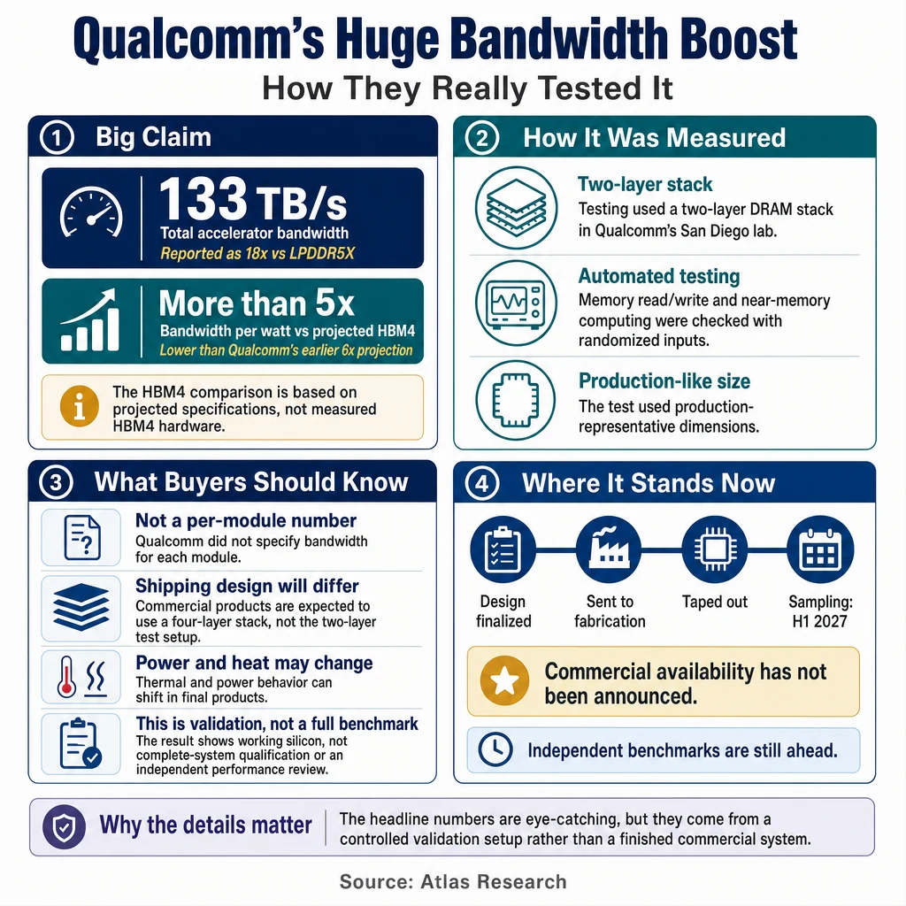
| Metric | Reported Figure | Measurement Context | Key Consideration for Buyers |
|---|---|---|---|
| Memory Bandwidth | 133 TB/s (18x vs LPDDR5X) | Total accelerator bandwidth, two-layer stack, San Diego lab | Per-module bandwidth not specified; production will use four-layer stack |
| Bandwidth per Watt | >5x HBM4 efficiency | Normalized to projected HBM4 specifications | Below Qualcomm's initial 6x projection; comparison is to estimated, not measured HBM4 |
| Test Configuration | Two-layer DRAM stack | Automated test equipment, randomized inputs, production-representative dimensions | Commercial products use four-layer stack; thermal/power characteristics will differ |
| Validation Type | Silicon validation | Memory read/write and near-memory computation functional testing | Not complete-system qualification or independent benchmark |
| Commercial Status | Taped out, sampling H1 2027 | Design finalized, sent to fabrication | Commercial availability unannounced; independent benchmarks ahead |
The data center infrastructure community now has evidence that Qualcomm's near-memory compute architecture functions as designed, with bandwidth and efficiency improvements that address genuine AI inference constraints. The specific numbers will be refined as the Dragonfly AI250 moves from validation to sampling to production. For now, practitioners should treat the 18x figure as a directional indicator of architectural potential rather than a procurement specification and watch for the independent benchmark data that will arrive with sample hardware in the first half of 2027.